PRESS RELEASES
Tomerdingen (Germany) - For immediate release - April 5, 2001
Boin GmbH, a software manufacturer for the semiconductor industry, has released version 2.0 of its metrology software WAFERMAP. The new version 2.0 now runs under Microsoft Windows 95, 98, NT 4.0 and 2000.
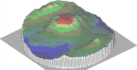
WAFERMAP is an award winning software package used to collect, edit, analyze and visualize measured physical parameters on semiconductor wafers. WAFERMAP can import data files from various metrology tools such as ellipsometers, thickness gauges and four point probes. The imported data can then be visualized or printed as line scans, contour plots, different 2D or 3D plots or as a histogram.
Several kinds of operations can be applied to the wafer maps such as rotation, shifting of the grid in the X or Y direction, or mirroring the data along the X or Y axis. Global operations such as adding or subtracting a constant or taking the 1st or 2nd derivative can be carried out. A Sigma Filter allows for the elimination of sites that exceed a user-defined range (e.g. measurement errors). In case of missing or invalid sites, a transformation to a standard circular or Cartesian grid can be performed. Different grids can be merged into a single new one. It is also possible to compare different sets of data by adding, subtracting or dividing entire wafer maps. Maps can be exported to ASCII data files.
Typical applications include map generation for manually operated metrology tools and standardized visualization for different automatic metrology equipment (e.g. different types of four point probes in the same fab). WAFERMAP allows users to work off-line and to analyze and edit metrology data outside of the clean room. It's the perfect solution for paperless fabs.
Version 2.0 adds a number of important new functions and capabilities to the software. Among them are:
- Transformation of grids (Cartesian, circular) keeping same measurement feature,
- Merge data of different files (e.g. two measurements of one wafer),
- Sigma Sorting Filter (1, 2, 3 sigma),
- Interpolation of sites,
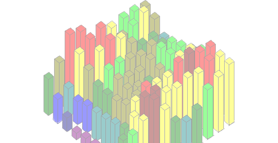
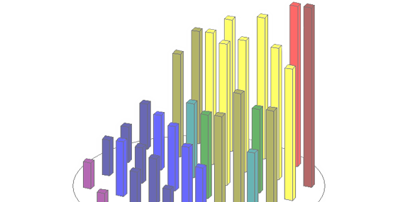
- 3D bar chart and 2D value plots,
- Calculation of Stacked Maps,
- Direct import of measurement files into the SPC tool,
- Statistical analysis and histogram for SPC values (Max, Min, Mean, ...) of all wafers.
Another important development has been incorporated into the software: the calculation of 1st and 2nd derivative of a map, regardless of the location and number of measurement sites. Also it is now possible to control WAFERMAP by Inter-application communication via DCOM (ActiveX server).
The software is already in use on a worldwide basis at a variety of IC and semiconductor equipment companies as well as wafer suppliers and research institutes. Among IC manufacturers, the software is used during production of analog, mixed-signal, DRAM and other integrated circuits including microprocessors and communications chips for the computer and telecommunications industries. It is used for production and testing of both silicon (Si) and gallium arsenide (GaAs) integrated circuits. Customers include LSI Logic, AMD, Infineon, KLA-Tencor, Philips, Sopra, Varian, Wacker Siltronic and others.
A free Evaluation Copy of WAFERMAP can be downloaded at Download.
Contact:
Boin GmbH, Dr. Manuela Boin
E-Mail: info@boin-gmbh.com
Web: www.boin-gmbh.com
Tel: +49 (0) 7348-928233