PRESS RELEASES
Tomerdingen (Germany) - For immediate release - August 12, 2003
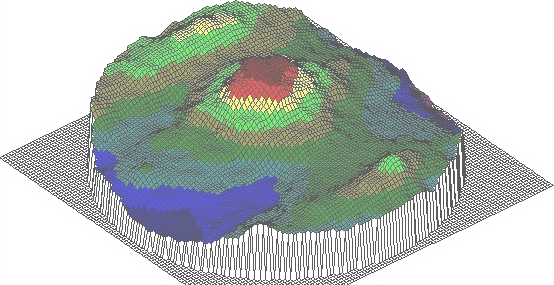
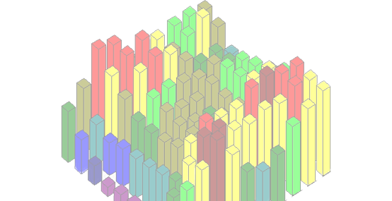
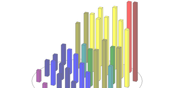
This year marks the 5th anniversary of a successful semiconductor software startup: Boin GmbH. The company was founded 5 years ago this August, when it introduced the WAFERMAP metrology software. WAFERMAP is an award winning software package used to collect, edit, analyze and visualize measured physical parameters on semiconductor wafers. WAFERMAP can import data files from various metrology tools such as ellipsometers, thickness gauges and four point probes. The imported data can then be visualized or printed as line scans, contour plots, 2D or 3D plots or as a histogram.
In March 2001 WAFERMAP-View.OCX, a software development kit for both the semiconductor and disk drive industry, was introduced. It offers the 7 different types of graphics of WAFERMAP as an ActiveX control. WAFERMAP-View.OCX employs an innovative object oriented visual programming interface to create and modify wafer plots. It was developed to satisfy the analysis and visualization needs of metrology equipment manufacturers.
Both software products broke new ground in two major areas. First, they enable process engineers to analyze and visualize metrology data from different automatic metrology equipment off-line, outside the clean room and in a standardized way. This makes such metrology data files easy comparable. A module for Statistical Process Control (SPC) is implemented offering trend charts, trend lists and an advanced file browser. WAFERMAP allows for a number of mathematical operations applied to metrology data files such as rotation, shifting of the grid in the X or Y direction, or mirroring the data along the X or Y axis. It is also possible to compare different sets of data by adding, subtracting or dividing entire wafer maps. Global operations such as adding or subtracting a constant or taking the 1st or 2nd derivative can be carried out. A Sigma Filter allows for the elimination of sites that exceed a user-defined range (e.g. measurement errors). In case of missing or invalid sites, a transformation to a standard circular or Cartesian grid can be performed. Different grids can be merged into a single new one. The WAFERMAP software is in use at a large number of IC and equipment manufacturers such as AMD, ASM, Infineon, KLA-Tencor, LSI Logic, Mattson, MEMC, Varian or Wacker Siltronic.
Second, both products have been integrated with a number of metrology tools in the semiconductor market and OEM agreements have been signed with manufaturers of metrology equipment. OEM customers such as Eichhorn & Hausmann, Foothill Instruments, Sigmatech, Sopra or Zeiss benefit from WAFERMAP and WAFERMAP-View.OCX by quick and easy integration into metrology applications and therefore save development time and costs.
The company has decided to donate 1% of its whole revenue in 2003 to fund children's education projects at UNICEF. The program started on January 1, 2003 and ends on December 31, 2003. Any order for WAFERMAP or WAFERMAP-View.OCX licenses, upgrades or other services received during this time period will take part in the program.
To visit the company's website go to www.boin-gmbh.com.
Contact:
Boin GmbH, Dr. Manuela Boin
E-Mail: info@boin-gmbh.com
Web: www.boin-gmbh.com
Tel: +49 (0) 7348-928233