PRESS RELEASES
Tomerdingen (Germany) - For immediate release - January 17, 2000
Carl Zeiss, a manufacturer of leading edge lithography systems for wafer steppers as well as inspection microscopes for defect classification and Boin GmbH, a metrology software manufacturer for the semiconductor industry, have signed an OEM agreement for the usage of Boin´s WAFERMAP software. The software will be used on Carl Zeiss´ Workstation Axiospeed FT PLUS to analyse and visualize film thickness measurements.
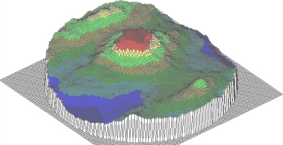
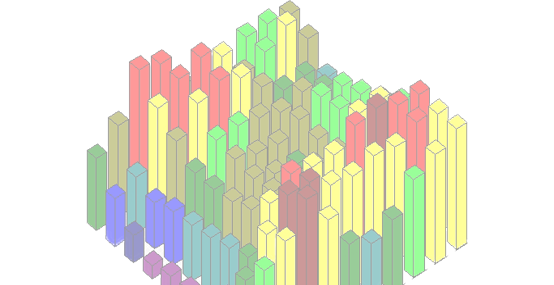
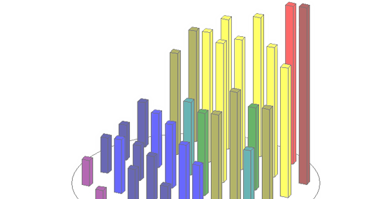
WAFERMAP, which runs under Windows 95 and NT4.0, allows for importing of data files from metrology equipment such as ellipsometers and four point probes as well as many other metrology tools used throughout the semiconductor industry. Data can be visualized and printed as 1D, 2D (contour) or 3D plots or as histograms.
Axiospeed FT PLUS is a system for automated film thickness measurement and mapping based on white light interference. The system uses a Zeiss diode array spectrometer and special evaluation software for measurement of transparent and semi transparentfilms in the range from 20 nm to about 100 µm. Basis of the workstation is the Zeiss inspection microscope Axiotron 2 with autofocus and high precision motor stage. Optionally the system can be equipped with wafer handling and pattern recognition for automatic positioning.
"We are glad to announce the cooperation with Carl Zeiss." said Dr. Manuela Boin, General Manager and co-founder of Boin GmbH. She added: "Focussing on OEM customers within the semiconductor equipment industry early in last year was the right decision for our company. We receive a strongly growing number of orders from this market segment."
"Visualization is a key issue for fast interpretation of measurement results." Hubert Jäger, product manager for Axiospeed FT PLUS pointed out. "WAFERMAP offers a wide choice of graphical presentations to the user and could easily be interfaced with the system software".
A free Evaluation Copy of WAFERMAP can be downloaded at Download.
Contact:
Boin GmbH, Dr. Manuela Boin
E-Mail: info@boin-gmbh.com
Web: www.boin-gmbh.com
Tel: +49 (0) 7348-928233
About Carl Zeiss:
Carl Zeiss is an innovative technology leader in the fields of optics and precision engineering. The Semiconductor Technology business group develops and produces leading edge lithography systems for wafer steppers as well as inspection microscopes for defect classification (up to 300mm wafers), mask simulation and inspection tools working at deep UV and 193nm wavelengths. The product spectrum extends from high resolution stand alone microscopes to high tech review and inspection systems with automatic defect classification software (ADC). Further information on Carl Zeiss may be obtained from the Internet at http://www.zeiss.de or by contacting the company directly.