PRESS RELEASES
Tomerdingen (Germany) - For immediate release - August 17, 2000
Boin GmbH, a software manufacturer for the semiconductor industry, announced today that its WAFERMAP software has gained its 50th customer after just under two years on the market. The software is already in use at a variety of IC and semiconductor equipment companies as well as wafer suppliers and research institutes worldwide. Among IC manufacturers the software is now used during production of silicon (Si) analog, mixed-signal, DRAM and other integrated circuits including microprocessors and communications chips for the personal computer industry as well as galliumarsenide (GaAs) integrated circuits.
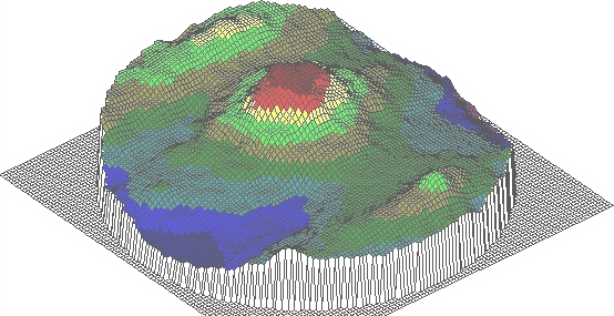
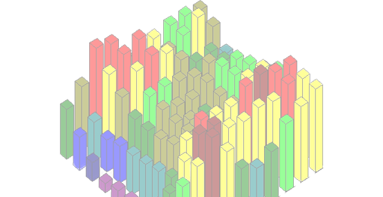
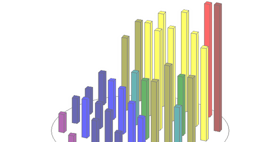
WAFERMAP is an award winning software package used to collect, edit, analyze and visualize measured physical parameters on semiconductor wafers. WAFERMAP can import data files from various metrology tools such as ellipsometers, thickness gauges and four point probes. The imported data can then be visualized or printed as line scans, contour plots, 2D or 3D plots or as a histogram. Several kind of of operations can be applied to the wafer maps such as rotation, shifting of the grid in the X or Y direction, or mirroring the data along the X or Y axis. It is also possible to compare different sets of data by adding, subtracting or dividing entire wafer maps. Maps can be exported to ASCII data files.
Dr. Manuela Boin, co-founder and General Manager of Boin GmbH said: "Since we are present in all major world regions with our distribution network we experienced a fast increase in the number of orders for WAFERMAP licenses." She added: "We received the majority of orders from fabs which are already in operation since more than one year. We expect to rapidly extend our base of customers during the next couple of months."
A free Evaluation Copy of WAFERMAP can be downloaded at Download.
Contact:
Boin GmbH, Dr. Manuela Boin
E-Mail: info@boin-gmbh.com
Web: www.boin-gmbh.com
Tel: +49 (0) 7348-928233