PRESS RELEASES
Tomerdingen (Germany) - For immediate release - May 20, 2002
Boin GmbH, a software manufacturer for the semiconductor industry, announced that it has shipped over 300 licenses of WAFERMAP, Boin's software for analyzing and visualizing of data files from metrology tools used in wafer fabs. In use by over 90 customers, WAFERMAP has become an important tool for IC and wafer manufacturers as well as metrology equipment suppliers.
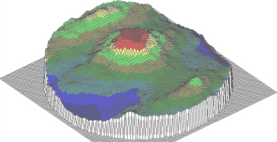
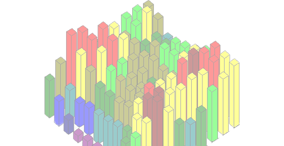
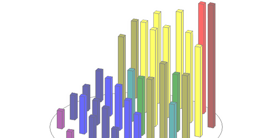
WAFERMAP is an award winning software package used to collect, edit, analyze and visualize measured physical parameters on semiconductor wafers. WAFERMAP can import data files from various metrology tools such as ellipsometers, thickness gauges and four point probes. The imported data can then be visualized or printed as line scans, contour plots, 2D or 3D plots or as a histogram. Among IC manufacturers, the software is used during production of analog, mixed-signal, DRAM and other integrated circuits including microprocessors and communications chips for the computer and telecommunications industries. It is used for production and testing of both silicon (Si) and gallium arsenide (GaAs) integrated circuits.
According to Dr. Manuela Boin, co-founder and General Manager of Boin GmbH, "The 300 license milestone firmly establishes WAFERMAP´s position as the premier tool to analyze and visualize metrology data in wafer fabrication, confirming its place as best tool for standardized visualization for different automatic metrology equipment."
A free Evaluation Copy of WAFERMAP can be downloaded at Download.
Contact:
Boin GmbH, Dr. Manuela Boin
E-Mail: info@boin-gmbh.com
Web: www.boin-gmbh.com
Tel: +49 (0) 7348-928233