|
Eichhorn & Hausmann - manufactures a wide range of measurement and handling systems for semiconductor wafers. They are all based on E + H's own special contactless capacitive sensor technology. Measurement applications include wafer thickness, geometry, resistivity and stress. |
 |
Filmetrics - is the industry leader in delivering affordable and easy-to-use thin-film instruments for measuring film thickness (30 Å to 450 μm), index of refraction, and film deposition rates. Systems available from UV to Visible to NIR wavelengths. Configurations available for tabletop, in-situ, and in-line applications. Filmetrics introduces affordability and ease-of-use to the semiconductor market. From robust, ultra-fast patterned wafer measurements to automated thickness mapping of unpatterned wafers for films up to 450 μm thick, Filmetrics delivers solutions for tabletop, integrated metrology, and fully automated cassette-to-cassette applications. |
 |
Foothill Instruments - manufactures film thickness metrology systems. The KT-22 table-top tool has been enhanced to measure the thickness of very thick films. Sample applications include advanced packaging, MEMS, and data storage. |
 |
Jordan Valley - with more than a quarter-century of advanced x-ray experience, Jordan Valley Semiconductors sets the standard in metrology solutions that deliver the accuracy, precision, and reliability required by high-volume fabs. Jordan Valley offers a comprehensive family of solutions based on advanced XRR and XRF technology. These tools are fully automated, production ready, and ideal for both blanket and patterned wafers. Jordan Valley's high-speed, non-destructive x-ray technology enables accurate and precise characterization of all film types including single layers and multilayer stacks, high k and low k materials, metals and dielectrics, amorphous, poly-crystal and single-crystal films. The powerful advantages delivered by the JVX™ system are backed by legendary reliability and support. No wonder Jordan Valley is the metrology solution approved by five of the world's top ten semiconductor manufacturers. |
 |
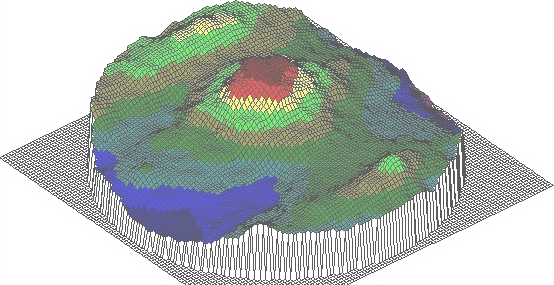
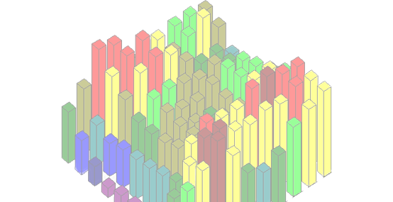
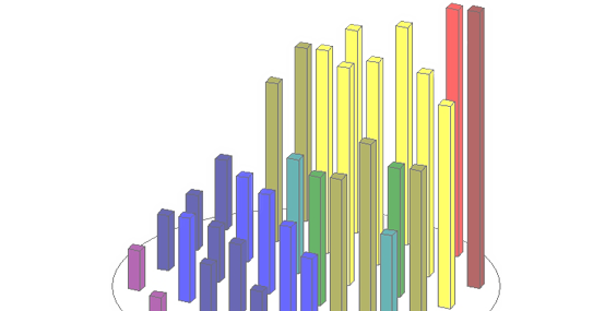
LayTec - is specialized on optical real-time process sensors for compound semiconductor epitaxy. These process sensors are capable of measuring growth rates, material composition, doping levels, and layer thickness both in MOCVD and MBE. A new product, the LayTec-MapR, measures the uniformity of film thickness, composition, doping level and roughness on wafers sized up to 300mm and communicates directly with Boin's WAFERMAP software. |
 |
SigmaTech - is a leading supplier of gauging equipment for the worldwide semiconductor industry. |
 |
SOPRA - SOPRA's ability to design and manufacture high quality metrology tools and analytical equipment with integrated mechanics, optics, electronics and software has become one of the company's key assets. |
 |
Tepla - is a manufacturer of laser-based metrology tools for the semiconductor industry. |
 |
Thermo - is a major supplier of portable and desktop analytical instrumentation and solutions to companies implementing compliance programs for their businesses. |
 |
Zeiss - offers a wide spectrum of high-quality products in the fields of optics, electronics and precision engineering. |
 |
Boin Blog - offers additional information and FAQs on WAFERMAP and PANELMAP. |